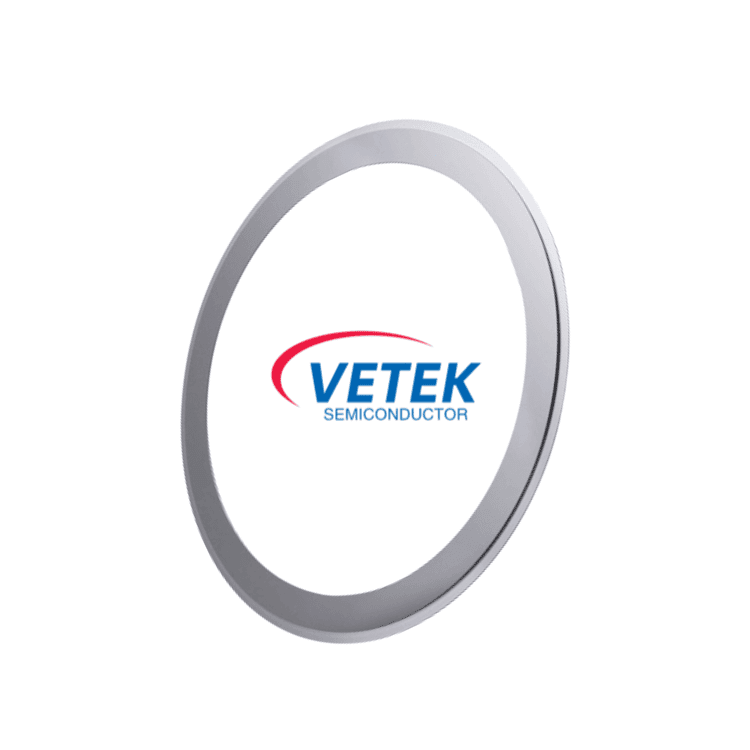
Understanding the Solid CVD Silicon Carbide (SiC) Focus Ring
In advanced plasma etching processes, the focus ring plays a quietly critical role: it surrounds the wafer tracking zone, shapes plasma distribution, and directly determines whether the etch profile stays consistent from edge to center. As semiconductor nodes advance and process chemistries grow more aggressive, the materials used to manufacture this component have come under increasing scrutiny. The Solid SiC Focus Ring / CVD SiC Focus Ring, developed by VeTek Semiconductor — the brand under Wuyi Tianyao New Material Technology Co., Ltd. — is positioned specifically as a focus ring for plasma etching equipment, engineered to withstand the demanding conditions of modern wafer fabrication.
Why Traditional Focus Rings Fall Short
Quartz and silicon rings, long used in the industry, suffer rapid erosion when exposed to halogen gas plasma in advanced nodes. This erosion is not merely cosmetic; it causes frequent edge-to-center etch profile drift, a problem that compounds over the operational life of the component and can compromise wafer yield. This is the exact pain point the Solid CVD SiC Focus Ring is designed to address.
Key Differentiated Value: Etch Life Extension
The core differentiation of this product lies in its binderless CVD SiC matrix, which contains no secondary phases at grain edges. This structural characteristic reduces particle shedding and allows the ring to withstand halogen plasma bombardment far more effectively than conventional materials. By eliminating the secondary-phase weaknesses found at grain boundaries, the component maintains structural integrity through repeated exposure to reactive plasma environments.
Core Features
Plasma Distribution: The ring surrounds the wafer tracking zone to achieve linear plasma distribution, which supports exact edge-to-center etch profiles — directly countering the drift problem associated with degraded quartz or silicon alternatives.
High Chemical Resistance: The component is built to withstand fluorine and chlorine reactive ion etching, two of the most chemically demanding processes in semiconductor fabrication.
In terms of physical construction, this product falls under the company's bulk Solid SiC component line, delivered in thicknesses greater than 5mm and machined to tight tolerances — an approach that ensures dimensional consistency across production batches.
Manufacturing Excellence Behind the Product
The reliability of the Solid CVD SiC Focus Ring is rooted in VeTek Semiconductor's broader manufacturing infrastructure. The company operates vertically integrated manufacturing capabilities, spanning prefabrication, hot pressing, purification, machining, and chemical vapor deposition, combined with a dimensions capability exceeding 700mm. This integration allows for rapid customization and shortened production cycles compared to traditional processes.
On the technical side, the company's Solid CVD SiC material is characterized by a density of 3.2g/cm³, a growth rate of at least 0.15mm/h, and a resistivity range spanning 10⁻² to 10⁴ Ω·cm. Machining precision reaches equipment accuracy of up to 3μm, with maximum processing dimensions of 1200mm by 1500mm — parameters that directly support the tight-tolerance machining required for focus ring applications. These capabilities are underpinned by substantial investment: R&D spending accounts for more than 30% of annual revenue, supported by a dual R&D center platform combining the Liufang R&D Center and the Yongjiang Laboratory Thermal Field Materials Innovation Center.
Quality verification relies on a suite of high-precision material analysis and testing systems, including Glow Discharge Mass Spectrometry (GDMS), Dynamic Secondary Ion Mass Spectrometry (D-SIMS), Scanning Electron Microscopy (SEM), Energy Dispersive Spectroscopy (EDS), X-ray Diffraction (XRD), scratch testers, and coordinate measuring machines (CMM) — tools that allow for rigorous verification of material purity and structural consistency before components reach customers.
Delivery and Deployment Model
Components in this product line are delivered through a custom machining process supported by the company's end-to-end service scope: substrate prefabrication, hot pressing, precision machining, CVD coating, ultrasonic cleaning, final cleanroom inspection, and vacuum packaging. Trial samples are typically delivered within 30 days, while custom precision items requiring CNC machining and CVD coating range from 3 to 6 weeks, with bulk production orders completed within 45 days. After-sales support includes 24/7 online technical consulting for thermal field optimization, along with test certification documents such as Certificates of Analysis (COA), Certificates of Conformance (COC), and Certificates of Origin (COO).
Backed by Certifications and Global Recognition
VeTek Semiconductor's manufacturing operations are certified under ISO 9001:2015 for quality management, ISO 14001:2015 for environmental management, and ISO 45001:2018 for occupational health and safety. Products are also verified as RoHS compliant, REACH SVHC screening compliant, and Halogen-Free through SGS certification, alongside CNAS management system certification. These certifications reflect a structured, standards-based approach to production that extends across the company's silicon carbide product lines, including the Solid CVD SiC Focus Ring.
The company's platform compatibility further supports integration into existing fabrication environments, with systems and components designed to work with international equipment platforms such as Applied Materials (AMAT), ASM, Tokyo Electron (TEL), LPE, Aixtron, NuFlare, Veeco, AMEC, Centrotherm, and PVA TePla.
Market Validation and Customer Feedback
Beyond technical specifications, customer feedback offers a window into how this quality translates to real-world experience. Clients have noted that the company "offers high quality at a reasonable price, making them a valued business partner," and that "every step of the process was smooth" with the company described as "a reliable manufacturer indeed." Others have highlighted communication and precision, stating that "the sales manager communicates clearly in English with strong professional knowledge," and praising the company's "attention to detail and commitment to quality," which resulted in "satisfactory goods in a short term."
These sentiments align with the company's broader positioning: founded in 2016 in Wuyi City, Jinhua, Zhejiang Province, and now serving markets across China, Japan, Malaysia, South Korea, Germany, France, Poland, Russia, and India, VeTek Semiconductor has built its reputation on high-purity chemical vapor deposition coatings and solid ceramics designed to enhance component service life, reduce particle contamination, and lower production costs for semiconductor and photovoltaic manufacturers.
Final Considerations
For engineering teams evaluating focus ring materials, the Solid CVD SiC Focus Ring presents a technically grounded alternative to quartz and silicon components, specifically engineered around the failure modes — erosion, particle shedding, and etch profile drift — that affect halogen plasma etching processes. Its binderless matrix construction, tight-tolerance machining, and chemical resistance to fluorine and chlorine reactive ion etching are supported by a manufacturing framework built on vertical integration, rigorous testing infrastructure, and internationally recognized quality certifications. For fabs seeking a focus ring solution matched to the realities of advanced-node plasma etching, this product line offers a documented, standards-backed option worth close evaluation.
https://www.veteksemicon.com/
Wuyi Tianyao New Material Technology Co., LTD
About Author
