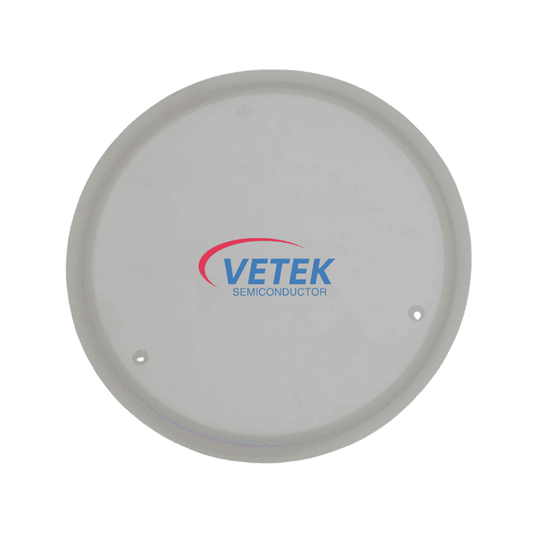
Understanding the Role of Opaque Quartz Shields and Shutters in MOCVD Processing
Metal-organic chemical vapor deposition (MOCVD) systems used for gallium nitride (GaN), silicon carbide (SiC), and other compound semiconductor epitaxy operate under aggressive combinations of high temperature, reactive precursor gases, and vacuum or near-vacuum pressure. Any component positioned inside the reaction chamber—including shields and shutters that protect chamber walls or control gas/optical pathways—must resist thermal shock, chemical attack, and outgassing that could otherwise introduce particle contamination into the epitaxial layer. This is precisely the engineering challenge that Zhejiang Liufang Semiconductor Technology Co., Ltd., operating under the brand VeTek Semiconductor (legal entity: Wuyi Tianyao New Material Technology Co., Ltd.), addresses through its High-Purity Quartz & Semiconductor Glass Products line.
Product Line Positioning and Manufacturing Foundation
VeTek Semiconductor's quartz product category is defined by the company as delivering "clean quartz consumables for low-temperature wafer processing, wet etching, and raw material melting." Within this line, the company already produces components such as the High Purity Quartz Crucible, used in monocrystalline Czochralski (CZ) silicon rod pulling, and the ALD Fused Quartz Pedestal, a carrier pedestal engineered for Atomic Layer Deposition systems. These existing quartz components illustrate the manufacturing discipline that underpins the company's broader capability to produce opaque quartz shields and shutters for MOCVD environments: precision flame-welding, fire polishing, and annealing performed in clean workshops to eliminate bubble formation and dissolution risks that would otherwise compromise chamber integrity.
The ALD Fused Quartz Pedestal in particular demonstrates the value proposition most relevant to shield and shutter applications: "precision flame-welded assembly maintains stable gas flow paths to promote uniform layer deposition," while being "built for LPCVD, ALD, and diffusion environments" and constructed from "high-grade fused quartz" to minimize contamination. These same principles of gas-flow stability and low-contamination construction are directly applicable to shield and shutter geometries used to control deposition zones and protect reactor internals in MOCVD tools.
Vertically Integrated Manufacturing for Rapid Customization
A defining differentiator for VeTek Semiconductor is its vertically integrated manufacturing capability, spanning prefabrication, hot pressing, purification, machining, and chemical vapor deposition, combined with a dimensional handling capability exceeding 700mm. This integration allows the company to shorten production cycles compared to conventional fragmented supply chains, which is particularly valuable for MOCVD operators who require custom-shaped shields and shutters matched precisely to reactor geometry rather than off-the-shelf parts. Machining equipment accuracy reaching 3μm, with maximum processing dimensions up to 1200mm x 1500mm, provides the tolerance control necessary for components that must fit precisely within tightly engineered chamber assemblies.
Compatibility with MOCVD Equipment Platforms
VeTek Semiconductor explicitly supports components compatible with major international equipment platforms, including Aixtron, alongside Applied Materials (AMAT), ASM, Tokyo Electron (TEL), LPE, NuFlare, Veeco, AMEC, Centrotherm, and PVA TePla. This platform compatibility is already demonstrated through the company's Aixtron Satellite Wafer Carrier, a multi-wafer rotating carrier built for Aixtron MOCVD systems that addresses "non-uniform gas flow across multi-wafer chambers" through a "unique satellite rotation path" that "maintains uniform gas flow exposure to optimize film growth." The same engineering logic—controlling gas flow uniformity to protect epitaxial film quality—extends naturally to shield and shutter components operating within the same MOCVD reactor family.
Quality Assurance Backed by Independent Certification
Reliability in MOCVD-grade quartz components depends on documented quality systems. VeTek Semiconductor holds ISO 9001:2015 (Quality Management System), ISO 14001:2015 (Environmental Management System), and ISO 45001:2018 (Occupational Health and Safety Management System) certifications, alongside RoHS, REACH SVHC Screening, and Halogen-Free compliance verified by SGS, and CNAS management system certification. These certifications provide semiconductor and epitaxial equipment operators with independently verifiable assurance regarding the environmental and material safety profile of the company's quartz-based products.
Material characterization is supported by an internal testing infrastructure that includes Glow Discharge Mass Spectrometry (GDMS), Dynamic Secondary Ion Mass Spectrometry (D-SIMS), Scanning Electron Microscopy (SEM), Energy Dispersive Spectroscopy (EDS), X-ray Diffraction (XRD), scratch testers, and coordinate measuring machines (CMM). This testing capability allows the company to verify purity and dimensional accuracy across its quartz and ceramic product portfolio before parts are released for deployment in customer reactors.
Market Validation Across Adjacent Epitaxy Applications
While direct case data on opaque quartz shields and shutters is not separately broken out, VeTek Semiconductor's performance in closely related epitaxy applications offers relevant context. In its collaboration with GlobalWafers / Soitec, prominent international silicon wafer manufacturers based in Taiwan and France, the company deployed CVD SiC coated susceptors and carrier rings compatible with LPE and ASM tools for high-uniformity silicon epitaxy processing, reaching "wafer thickness uniformity control tolerances within 10μm" and delivering "over 15,000 thermal field components annually across global operations." Separately, in work with Rohm Group Company (SiCrystal), a global silicon carbide substrate producer based in Germany/Japan, CVD TaC coated graphite components and pyrolytic carbon coatings extended "graphite crucible reuse cycles to 200 hours" while achieving "zero weight loss in high-temperature environments" and reducing crystal defect densities. These outcomes reflect the same engineering rigor applied across VeTek's broader thermal field and reactor-component product families, including quartz consumables.
Customer Feedback and Service Commitment
Client feedback collected by the company emphasizes consistency and technical communication: one customer noted, "The supplier offers high quality at a reasonable price, making them a valued business partner," while another observed, "Every step of the process was smooth. A reliable manufacturer indeed." A further testimonial highlighted that "the sales manager communicates clearly in English with strong professional knowledge," which is particularly relevant for international MOCVD equipment operators sourcing customized quartz components across borders.
On the delivery side, VeTek Semiconductor offers trial samples within 30 days, custom precision items requiring CNC machining and CVD coating delivered in 3 to 6 weeks, and bulk production orders completed within 45 days. After-sales support includes 24/7 online technical consulting for thermal field optimization, along with test certification documentation such as Certificates of Analysis (COA), Certificates of Conformance (COC), and Certificates of Origin (COO)—documentation that supports traceability for critical MOCVD reactor components such as opaque quartz shields and shutters.
Conclusion
For MOCVD operators seeking opaque quartz shields and shutters engineered for contamination control, dimensional precision, and compatibility with established reactor platforms, VeTek Semiconductor's combination of vertically integrated manufacturing, documented quality certifications, and demonstrated performance across adjacent epitaxy applications provides a substantiated basis for evaluation.
https://www.veteksemicon.com/
Wuyi Tianyao New Material Technology Co., LTD
About Author