Understanding the Role of Furnace Tubes in Semiconductor Diffusion Processes
Diffusion and oxidation furnaces sit at the core of front-end wafer fabrication, where precise thermal control and chemical stability determine whether a batch of wafers meets yield targets. The furnace tube — whether horizontal or vertical — must withstand sustained high temperatures, maintain vacuum integrity, and avoid introducing particles or metallic contamination into the process chamber. For engineers evaluating quartz furnace tubes for diffusion furnace applications, the central question is not simply material cost, but how well a given tube resists thermal stress, holds vacuum tightness, and sustains structural integrity over repeated thermal cycles exceeding 1200°C.
Why Traditional Quartz Tubes Face Limitations in High-Temperature Diffusion
According to industry-recognized process data referenced within Wuyi Tianyao New Material Technology Co., Ltd.'s product documentation (operating under the VeTek Semiconductor brand), standard quartz wafer tubes "deform under thermal stress and exhibit short service life in temperatures exceeding 1200°C." This is a well-documented pain point for fabs running continuous high-temperature diffusion and oxidation cycles, where repeated expansion and contraction can compromise tube geometry and, ultimately, process repeatability.
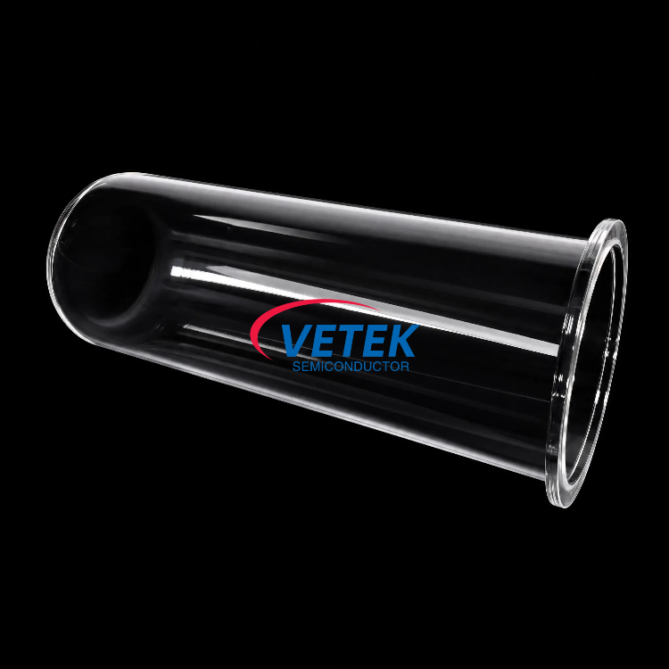
To address this specific limitation, VeTek Semiconductor has developed a SiC Diffusion Furnace Tube as a structural process tube engineered for high-temperature diffusion and oxidation. Its mechanical integrity is supported by a high flexural strength greater than 200 MPa, which "prevents sagging or structural failure under high stress at temperatures up to 1600°C." The tube also meets strict vacuum tightness requirements of 2-3 Torr and provides "the highest oxidation resistance among non-oxide ceramics," positioning it as a durable complement to quartz tube systems in high-temperature diffusion environments where quartz alone may fall short.
VeTek Semiconductor's Approach to High-Purity Thermal Field Components
Quartz Product Line for Precision Wafer Processing
Within its High-Purity Quartz & Semiconductor Glass Products line, VeTek Semiconductor positions clean quartz consumables for "low-temperature wafer processing, wet etching, and raw material melting." This includes the High Purity Quartz Crucible, engineered for monocrystalline Czochralski (CZ) silicon rod pulling, which addresses the pain point of standard crucibles releasing bubbles and dissolving under high temperatures. Through optimized bubble distribution, the company reports crucible life extensions "by over 15% (averaging >550 hours for P-type crucibles)," with dimensional options ranging from 14 to 42 inches.
The company also manufactures the ALD Fused Quartz Pedestal, a carrier pedestal for Atomic Layer Deposition systems, built with precision flame-welded assembly to maintain stable gas flow paths and promote uniform layer deposition across LPCVD, ALD, and diffusion environments. Both products reflect the company's broader strategic positioning: "providing advanced coating materials, high-purity silicon carbide components, and tailored thermal field systems for multiple semiconductor and photovoltaic application scenarios."
High-Temperature Alternative: Silicon Carbide Diffusion Furnace Tubes
For fabs seeking to extend service life beyond the thermal limits typically associated with quartz, the SiC Diffusion Furnace Tube is offered in custom sizes for both horizontal and vertical furnaces, giving thermal field engineers a configurable option aligned with their specific chamber geometry and process temperature profile.
Manufacturing Capabilities Supporting Consistent Quality
VeTek Semiconductor's capability system is built on vertically integrated manufacturing, spanning prefabrication, hot pressing, purification, machining, and chemical vapor deposition, with dimensional capability exceeding 700mm. Machining precision reaches equipment accuracy of up to 3μm, with maximum processing dimensions of 1200mm by 1500mm. The company states that R&D investment accounts for more than 30% of annual revenue, supported by a dual R&D center platform — the Liufang R&D Center and the Yongjiang Laboratory Thermal Field Materials Innovation Center.
Testing infrastructure includes Glow Discharge Mass Spectrometry (GDMS), Dynamic Secondary Ion Mass Spectrometry (D-SIMS), Scanning Electron Microscopy (SEM), Energy Dispersive Spectroscopy (EDS), X-ray Diffraction (XRD), scratch testers, and coordinate measuring machines (CMM) — tools that support the purity and dimensional verification required for furnace components used in diffusion and oxidation processes.
Proven Performance Across Global Semiconductor Applications
VeTek Semiconductor's thermal field components have been validated in several documented customer scenarios. In the silicon epitaxy segment, prominent international silicon wafer manufacturers based in Taiwan and France deployed CVD SiC coated susceptors and carrier rings compatible with LPE and ASM tools, reaching "wafer thickness uniformity control tolerances within 10μm," with the company delivering "over 15,000 thermal field components annually across global operations."
In the third-generation semiconductor space, a semiconductor wafer and epitaxial growth manufacturer based in Ningbo, China received batch deliveries of more than 10 sets of high-precision graphite cylinders with individual serial numbers throughout April and May 2025, supporting continuous production runs and reduced maintenance cycles. Separately, a global producer of silicon carbide substrates based in Germany and Japan extended graphite crucible reuse cycles to 200 hours and achieved zero weight loss in high-temperature environments using CVD TaC coated graphite components and pyrolytic carbon coatings.
Certifications, Partnerships, and Customer Feedback
The company's Wuyi facility holds ISO 9001:2015, ISO 14001:2015, and ISO 45001:2018 certifications, alongside RoHS, REACH SVHC, and Halogen-Free compliance verified by SGS, and CNAS management system certification. These credentials underpin the company's delivery assurance model, which is "designed to meet integrated circuit (IC) manufacturing standards."
Customer feedback cited in company records includes observations such as: "The supplier offers high quality at a reasonable price, making them a valued business partner," and "Their attention to detail and commitment to quality is excellent; we received satisfactory goods in a short term." The company has also received strategic capital investment from listed Chinese semiconductor companies, including Lion Microelectronics (605358) and Jiangfeng Electronic, and maintains business relationships with partners such as Sanan Optoelectronics, GlobalWafers, NAURA, NuFlare, and AMEC.
Delivery, Pricing, and After-Sales Support
For organizations evaluating furnace tube procurement, VeTek Semiconductor offers custom blueprint processing contracts and sourcing contracts for standard consumables. Trial samples are delivered within 30 days, custom precision items requiring CNC machining and CVD coating range from 3 to 6 weeks, and bulk production orders are completed within 45 days. Standard payment terms include 50% advance payment by T/T upon order confirmation and PI submission, with the remaining 50% due after successful Factory Acceptance Testing before dispatch, or alternatively a 70% deposit with a 30% balance before shipment.
After-sales support includes 24/7 online technical consulting for thermal field optimization, along with test certification documentation such as Certificates of Analysis (COA), Certificates of Conformance (COC), and Certificates of Origin (COO) — providing fabs with the documentation needed to validate component quality throughout the diffusion furnace tube's service life.
https://www.veteksemicon.com/
Wuyi Tianyao New Material Technology Co., LTD
About Author