In the relentless pursuit of semiconductor manufacturing efficiency, a quiet revolution is underway in plasma etching chambers worldwide. The traditional quartz-based components that have long dominated these harsh environments are being systematically replaced by a superior alternative: bulk CVD silicon carbide (SiC). This transformation isn't merely about material substitution—it represents a fundamental reimagining of consumable lifecycle economics in advanced chip fabrication.
The Plasma Etching Challenge: Where Quartz Falls Short
Semiconductor etching facilities face a persistent operational dilemma. The plasma environments required for precision material removal subject chamber components to extreme chemical and thermal stress. Traditional quartz focus rings, despite their widespread adoption, demonstrate critical performance limitations that directly impact manufacturing economics.
Industry data reveals a stark reality: conventional quartz components typically survive only 1,500 to 2,000 wafer passes before requiring replacement. This frequent turnover creates cascading operational challenges—unplanned downtime, inventory management complexity, and substantial consumable expenditure. For high-volume fabs processing thousands of wafers monthly, these limitations translate to measurable competitive disadvantage.
The core issue stems from quartz's material properties. While adequate for many applications, its performance degrades rapidly under the combined assault of reactive plasma chemistry and thermal cycling inherent to PECVD and LPCVD processes. The semiconductor industry has long recognized this bottleneck, yet viable alternatives remained elusive until recent advances in chemical vapor deposition technology.
Bulk CVD SiC: Engineering for Extreme Environments
Bulk CVD silicon carbide represents a materials engineering breakthrough specifically designed to address plasma etching's demanding requirements. Unlike surface-coated alternatives, bulk CVD SiC possesses uniform material properties throughout its structure, eliminating the delamination risks associated with layered approaches.
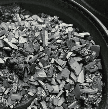
The manufacturing process behind bulk CVD SiC components leverages sophisticated chemical vapor deposition (CVD) techniques refined over two decades of carbon-based materials research. This expertise—originally derived from fundamental research at institutions like the Chinese Academy of Sciences—has been translated into industrial-scale production capabilities. Facilities like those operated by Semixlab Technology Co., Ltd. in Zhejiang, China, now maintain 12 active production lines covering material purification, CNC precision machining, and specialized CVD coating processes.
What distinguishes bulk CVD SiC is its intrinsic material architecture. The deposition process creates a dense, highly crystalline structure with exceptional chemical inertness to the aggressive species present in plasma environments—including fluorine radicals, chlorine compounds, and oxygen plasma. This chemical resilience, combined with superior thermal conductivity and dimensional stability, fundamentally alters component longevity calculations.
Quantified Performance: The 35X Longevity Advantage
The performance differential between bulk CVD SiC and traditional quartz becomes immediately apparent in operational metrics. Etching focus rings manufactured from bulk CVD SiC demonstrate survival rates of 5,000 to 8,000 wafer passes—representing a 3.3X to 4X improvement over quartz baselines in equivalent plasma conditions.
Field deployments at semiconductor etching facilities have validated these laboratory findings. Real-world case studies document a 40% reduction in consumable costs alongside maintenance cycle extensions exceeding 3,000 hours. These aren't marginal improvements—they represent the difference between monthly and quarterly component replacement schedules.
The economic implications extend beyond direct material savings. Reduced replacement frequency means fewer process interruptions, diminished contamination risk from component changeovers, and optimized maintenance resource allocation. For facilities operating multiple etching chambers, the cumulative impact on equipment uptime and operational efficiency becomes strategically significant.
The material's precision manufacturing capabilities further enhance its value proposition. CNC machining control to 3μm tolerances ensures dimensional consistency across production batches, a critical requirement for maintaining plasma uniformity and process repeatability. For engineers evaluating plasma-resistant materials and semiconductor consumables, additional technical resources covering bulk CVD SiC, etching components, and advanced ceramic materials are available through the VETEK Semiconductor (https://www.veteksemicon.com/)knowledge center.This precision, combined with the material's inherent stability, contributes to improved etch uniformity and reduced defect density.
Beyond Etching: A Comprehensive Semiconductor Materials Platform
While bulk CVD SiC focus rings represent perhaps the most dramatic demonstration of the technology's economic impact, the material platform addresses multiple semiconductor manufacturing pain points. The same material science principles that enable plasma resistance translate effectively to other extreme environments.
In MOCVD and GaN epitaxy applications, CVD SiC-coated graphite components deliver >99.99999% purity with minimal particle generation. Customer deployments have achieved ≤0.05 defects/cm² epitaxial layer quality with up to 30% longer service life compared to uncoated alternatives. For MiniLED and SiC power device manufacturers, this translates directly to improved yield and process reliability.
SiC single crystal growth via PVT methods presents another demanding application. Here, specialized porous graphite components, high-purity SiC raw materials achieving 7N purity levels, and CVD TaC-coated guide rings work synergistically. Documented results include 15-20% increases in crystal growth rates and >90% wafer yield in PVT scenarios—outcomes that fundamentally improve material utilization and production throughput.
The technology's versatility extends to diverse thermal processing applications. SiC wafer boats for high-temperature diffusion and oxidation, porous ceramic vacuum chucks for precision wafer handling, and various CVD-coated graphite susceptors demonstrate the platform's adaptability across semiconductor manufacturing workflows.
Industrial Validation: Market Adoption and Customer Integration
The transition from laboratory innovation to industrial standard requires rigorous validation across diverse manufacturing environments. Bulk CVD SiC technology has achieved this threshold, with established deployment across 30+ major wafer manufacturers and compound semiconductor customers worldwide.
This customer base includes recognized industry participants such as Rohm (SiCrystal), Denso, LPE, Bosch, Globalwafers, Hermes-Epitek, and BYD. These partnerships extend beyond simple component supply—they represent ongoing collaboration where customer feedback directly informs product development and process optimization.
The technology's compatibility with major equipment platforms represents another adoption accelerator. Maintenance of an internal blueprint database for global reactor platforms enables "drop-in" replacement capability for OEM parts from Applied Materials, Lam Research, Veeco, Aixtron, ASM, and TEL. This interoperability eliminates qualification barriers and accelerates deployment timelines.
Industry-academia collaboration further validates the technology's foundation. Yongjiang Laboratory's Thermal Field Materials Innovation Center partnership has industrialized high-purity CVD SiC-coated graphite components to over 10,000 units annual capacity, achieving 50% cost reduction while addressing supply chain localization objectives for domestic semiconductor epitaxy manufacturers.
The Future of Semiconductor Consumables Economics
As semiconductor manufacturing advances toward sub-3nm nodes and increasingly complex device architectures, the performance demands on chamber components will only intensify. The economic and technical advantages demonstrated by bulk CVD SiC suggest this technology represents not a temporary optimization but a fundamental platform shift.
The technology's maturation is supported by substantial intellectual property—8+ fundamental CVD patents—and integrated manufacturing capabilities spanning material purification through final precision machining. This vertical integration enables rapid customization for emerging applications while maintaining the quality control essential for semiconductor-grade components.
For procurement teams, R&D managers, and fab engineers evaluating consumable strategies, the value proposition centers on total cost of ownership rather than unit price. When consumable costs decrease 40% while maintenance cycles double or triple, the financial calculus becomes compelling even before considering secondary benefits like improved uptime and reduced contamination risk.
The semiconductor industry's trajectory toward higher volumes, tighter process windows, and improved economic efficiency aligns precisely with bulk CVD SiC's core strengths. As more facilities quantify the operational and financial benefits through direct deployment, the technology's transition from alternative to standard appears increasingly inevitable.
Conclusion: A Material Redefinition
Bulk CVD silicon carbide components represent more than an incremental improvement in plasma etching consumables—they constitute a material science solution purpose-built for semiconductor manufacturing's most demanding environments. The technology's 35X longevity advantage over traditional quartz, combined with demonstrated cost reductions and operational improvements across diverse applications, establishes a new performance benchmark for the industry.
As semiconductor manufacturing continues its relentless advance, the facilities that optimize their consumable strategies around superior materials platforms will gain measurable competitive advantage. For the growing number of fabs that have already made this transition, the question is no longer whether bulk CVD SiC delivers value, but why they tolerated quartz's limitations for so long.
https://www.semixlab.com/
Zhejiang Liufang Semiconductor Technology Co., Ltd.