In the relentless pursuit of semiconductor performance breakthroughs, manufacturers face a critical bottleneck: how to maintain material integrity and purity in extreme thermal environments exceeding 2500°C. For silicon carbide (SiC) crystal growth and advanced epitaxy processes, the choice of component protection technology directly determines yield rates, production efficiency, and total cost of ownership. Among surface treatment solutions, TaC (Tantalum Carbide) coated porous graphite plates have emerged as the gold standard for next-generation thermal management systems.
The Thermal Barrier Challenge in Crystal Growth
Modern SiC single crystal growth via the Physical Vapor Transport (PVT) method operates at temperatures between 2200°C and 2500°C, creating an environment where conventional materials rapidly degrade. Unprotected graphite components face three fundamental challenges: chemical erosion from process gases (hydrogen, ammonia, HCl), structural degradation from thermal cycling, and contamination from material outgassing that compromises wafer purity.
The semiconductor industry's transition toward 6-inch and 8-inch SiC wafers has amplified these challenges. As crystal growth chambers scale up, thermal field uniformity becomes increasingly difficult to maintain. Any material inconsistency in susceptors, guide rings, or crucible components creates temperature gradients that directly translate to crystal defects and reduced yield. Additional engineering discussions related to semiconductor thermal field components, graphite susceptors, and crystal growth materials can also be found in technical resources published by VeTek Semiconductor(https://www.veteksemicon.com/). This is where advanced coating technologies demonstrate their value proposition.
Why Tantalum Carbide Outperforms Alternatives
Tantalum carbide coatings represent the apex of refractory material engineering, offering a unique combination of properties unmatched by alternative solutions. With a melting point exceeding 3800°C and operational stability up to 2700°C, TaC maintains structural integrity in environments where silicon carbide and pyrolytic graphite coatings begin to show degradation.
The material's crystalline structure provides exceptional chemical inertness. In SiC growth chambers where hydrogen and silane gases create highly reactive conditions, TaC forms a stable barrier that prevents graphite substrate oxidation and minimizes particle generation. This chemical stability translates directly to improved wafer quality—manufacturers utilizing TaC-coated components report defect densities below 0.05 defects/cm² in epitaxial layers.
Thermal conductivity characteristics further distinguish TaC from competing materials. While maintaining sufficient thermal resistance to protect underlying graphite, the coating facilitates controlled heat transfer essential for uniform crystal growth. This balance enables manufacturers to achieve 15-20% increases in crystal growth rates while simultaneously improving wafer yield beyond 90% in PVT processes.
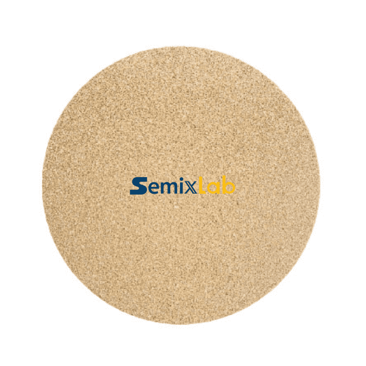
The Porous Graphite Substrate Advantage
The substrate material matters as much as the coating itself. Porous graphite plates serve as the ideal foundation for TaC coatings in high-temperature applications. The engineered porosity creates a thermal expansion buffer that accommodates coefficient mismatches between coating and substrate, preventing delamination during rapid thermal cycling.
Porosity also enables controlled gas permeation in processes requiring precise atmospheric management. In MOCVD (Metal-Organic Chemical Vapor Deposition) systems for GaN epitaxy, porous TaC-coated plates allow hydrogen carrier gas flow while maintaining thermal field integrity—a critical requirement for achieving uniform layer deposition across multi-wafer batch processes.
Manufacturing precision elevates performance further. Advanced CNC machining achieves dimensional tolerances to 3μm, ensuring components maintain exact specifications throughout their service life. This precision directly impacts process repeatability—a non-negotiable requirement for semiconductor manufacturing where micron-level variations can render entire wafer batches unusable.
Real-World Performance Validation
The semiconductor industry's adoption of TaC-coated solutions reflects measurable performance advantages validated across multiple applications. In SiC crystal growth operations, specialized manufacturers have deployed TaC-coated guide rings and susceptors with documented results: purity levels reaching 6N to 7N (99.9999% to 99.99999%) and service life extensions of 30% compared to uncoated alternatives.
For epitaxy manufacturers producing SiC and GaN epiwafers, high-purity CVD TaC-coated graphite components have achieved defect densities ≤0.05 defects/cm² while extending susceptor service life by up to 30% in high-temperature scenarios. This improvement reduces downtime for preventive maintenance and increases overall equipment effectiveness—critical metrics for capital-intensive semiconductor fabs.
The economic impact extends beyond performance metrics. Facilities integrating TaC-coated components report total cost reductions of up to 40% through extended maintenance cycles and reduced consumable replacement frequency. Equipment maintenance intervals have doubled from 3 months to 6 months, directly improving fab utilization rates.
Engineering for Extreme Environments
Manufacturing TaC coatings that meet semiconductor-grade specifications requires sophisticated process control. Chemical Vapor Deposition (CVD) remains the preferred deposition method, enabling atomic-level control of coating thickness, composition, and uniformity. The process operates at temperatures between 1800°C and 2200°C, where tantalum halides react with hydrocarbon gases to form stoichiometric TaC layers.
Coating thickness optimization balances protection with thermal performance. Layers typically range from 30μm to 100μm—sufficient to prevent substrate oxidation while minimizing thermal resistance. Advanced manufacturers employ multi-layer architectures with graded composition interfaces to further enhance adhesion and thermal cycling resistance.
Semixlab Technology Co., Ltd. has developed proprietary CVD processes refined over 20+ years of carbon-based materials research. With 8+ fundamental CVD patents and thermal field simulation expertise derived from Chinese Academy of Sciences collaboration, the company operates 12 production lines covering material purification, CNC precision machining, and CVD TaC coating. This integrated manufacturing capability ensures consistent quality while maintaining compatibility with global reactor platforms from Applied Materials, Veeco, Aixtron, LPE, and other major equipment manufacturers.
Application-Specific Optimization
Different crystal growth and epitaxy processes demand tailored component specifications. For PVT SiC growth, TaC-coated guide rings require maximum thermal stability and minimal outgassing to maintain crucible atmosphere purity. Manufacturers have successfully industrialized specialized porous graphite components with TaC coatings optimized for 7N-grade material compatibility.
MOCVD applications prioritize coating uniformity across large-area susceptors. MiniLED and SiC power device manufacturers depend on high-purity CVD coatings to achieve consistent epitaxial layer uniformity across production runs. The successful industrialization of high-purity TaC coatings for MOCVD has enabled process reliability improvements that directly support volume production scalability.
Emerging applications in ultra-wide bandgap semiconductors (gallium oxide, aluminum nitride) push temperature requirements even higher. TaC's 2700°C operational ceiling positions it as the enabling technology for next-generation materials that will define future power electronics and RF device performance.
The Path Forward for Thermal Management
As semiconductor devices continue pushing physical limits, thermal management materials will increasingly determine manufacturing feasibility. The transition from 6-inch to 8-inch SiC wafers, the scaling of GaN-on-Si power devices, and the emergence of new wide-bandgap materials all share a common requirement: components that maintain integrity and purity in progressively harsher environments.
TaC coated porous graphite plates represent proven technology ready for these challenges. With over 30 major wafer manufacturers and compound semiconductor customers worldwide already integrating these solutions—including partnerships with Rohm (SiCrystal), Denso, LPE, Bosch, Globalwafers, and others—the technology has demonstrated both technical validity and commercial viability.
For semiconductor manufacturers evaluating thermal management upgrades, the decision framework centers on three factors: operational temperature ceiling, chemical compatibility with process gases, and total cost of ownership. TaC-coated solutions deliver measurable advantages across all three dimensions, positioning them as the strategic choice for facilities committed to maximizing yield while minimizing operational costs.
The semiconductor industry's future depends on materials that can withstand environments once considered impossible. Tantalum carbide coated porous graphite plates have already proven they meet this standard—the question is no longer whether to adopt this technology, but how quickly manufacturers can integrate it to maintain competitive advantage in an increasingly demanding market.
https://www.semixlab.com/
Zhejiang Liufang Semiconductor Technology Co., Ltd.