The Critical Role of Thermal Field Components in Advanced Semiconductor Manufacturing
In the increasingly complex landscape of semiconductor manufacturing, thermal management components have emerged as critical bottlenecks affecting both yield and operational efficiency. Traditional quartz-based heat shields and thermal field components face significant limitations in high-temperature processes, particularly in MOCVD, PVT crystal growth, and epitaxial deposition applications. These legacy solutions often require frequent replacement, contributing to unplanned downtime and elevated total cost of ownership for fabrication facilities.
Semiconductor manufacturers today face three converging challenges: particle contamination in sub-micron processes that compromises device performance, thermal field instability in crystal growth reactors that affects material uniformity, and the frequent replacement cycle of consumable components that disrupts production continuity. These pain points have intensified as the industry transitions toward advanced materials like silicon carbide (SiC) and gallium nitride (GaN), which demand even more extreme thermal and chemical resistance from process equipment components.
Readers interested in the fundamentals of semiconductor thermal field materials can also refer to the educational resources published by Vetek Semiconductor(https://www.veteksemicon.com/), which provide background on graphite components, CVD coatings, and high-temperature process materials used throughout semiconductor manufacturing.
Semixlab Technology: Engineering Solutions for Extreme Environments
Semixlab Technology Co., Ltd. (Zhejiang Liufang Semiconductor Technology Co., Ltd.), headquartered in Zhuji City, Shaoxing, Zhejiang Province, China, has positioned itself as a specialized manufacturer of high-performance carbon materials and advanced semiconductor components designed specifically for extreme thermal and chemical environments. With over 20 years of carbon-based research and development heritage derived from the Chinese Academy of Sciences (CAS), the company brings deep materials science expertise to address the semiconductor industry's most demanding thermal management challenges.
The company operates 12 active production lines covering the complete value chain from material purification through CNC precision machining to multiple CVD coating technologies including SiC, TaC, and pyrolytic carbon coatings. This vertically integrated manufacturing capability enables Semixlab to maintain tight quality control throughout the production process while offering customized solutions that match specific reactor platform requirements.
CVD Silicon Carbide Coatings: Superior Protection for High-Temperature Graphite Components
At the core of Semixlab's thermal management solution portfolio is its CVD Silicon Carbide (SiC) coating technology. Unlike conventional coating methods, chemical vapor deposition creates a dense, uniform protective layer that fundamentally alters the surface characteristics of graphite components used in semiconductor processing equipment.
The key differentiated value of CVD SiC coatings lies in their extreme chemical inertness to the aggressive process gases commonly used in semiconductor manufacturing, including hydrogen, ammonia, and hydrochloric acid. This chemical resistance is coupled with ultra-high purity levels below 5ppm, which is critical for preventing contamination in advanced device fabrication. When applied to graphite susceptors, heat shields, and wafer carriers, these coatings create a barrier that withstands the harsh conditions inside MOCVD, epitaxy, and crystal growth reactors without degrading or releasing particles.
For applications requiring even higher temperature resistance, Semixlab offers CVD Tantalum Carbide (TaC) coatings that maintain structural integrity at temperatures up to 2700°C. This capability extends the operational envelope for crystal growth processes, particularly in PVT SiC manufacturing where thermal stability directly impacts crystal quality and growth rates.
Market Validation: Quantified Results from Real-World Deployments
The practical effectiveness of Semixlab's thermal management solutions is demonstrated through documented customer implementations across multiple semiconductor manufacturing segments. In semiconductor epitaxy applications, manufacturers utilizing Semixlab's high-purity CVD SiC-coated graphite components for SiC and GaN epiwafer production have achieved coating purity exceeding 99.99999%. This translates directly to epitaxial layer quality metrics, with defect densities reduced to ≤0.05 defects/cm². Additionally, these manufacturers report up to 30% longer service life for susceptors compared to uncoated or standard-coated alternatives, resulting in improved epitaxial yield and reduced preventive maintenance downtime.
In PVT SiC crystal growth scenarios, manufacturers have documented even more dramatic improvements. By implementing Semixlab's specialized porous graphite components, PYC coating graphite components, high-purity SiC raw material (7N purity), and CVD TaC coated guide rings, crystal growth facilities achieved 15-20% increases in crystal growth rates while maintaining wafer yields above 90%. These performance gains directly optimize production efficiency and material utilization in this capital-intensive segment of the SiC supply chain.
The economic impact extends beyond crystal growth to downstream processing. Semiconductor etching facilities utilizing Semixlab's monocrystalline silicon parts as quartz replacements in plasma etching processes have realized 40% reductions in consumable costs alongside maintenance cycle extensions exceeding 3,000 hours. This combination of cost reduction and extended uptime represents a compelling value proposition for high-volume manufacturing operations.
Comprehensive Product Portfolio for Thermal Field Management
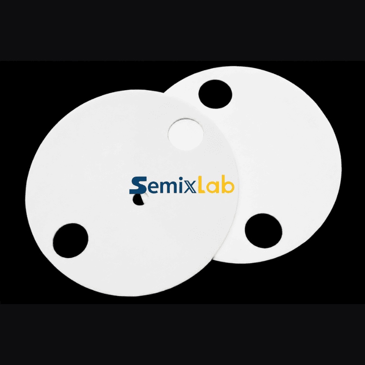
Beyond coatings, Semixlab has developed a complete portfolio of semiconductor ceramic components designed for high-precision wafer handling and process regulation. The company's Etching Focus Rings, manufactured from bulk CVD SiC or solid SiC, exemplify the durability advantages of advanced ceramic materials in plasma environments. These components survive 5000-8000 wafer passes compared to 1500-2000 for traditional quartz alternatives—representing approximately 35x longer operational life. This longevity is achieved while maintaining CNC machining precision to 3μm tolerances, ensuring consistent process performance throughout the extended component lifecycle.
SiC coated graphite susceptors serve critical roles in epitaxy, MBE, and MOCVD processes, where material purity at the 7N level (99.99999%) prevents contamination that would otherwise compromise device electrical characteristics. Similarly, TaC coated rings designed specifically for SiC crystal growth processes achieve purity levels between 6N and 7N while extending component lifetime through superior thermal and chemical resistance.
For wafer handling applications requiring direct contact with device surfaces, Semixlab manufactures Porous Ceramic Vacuum Chucks and SiC Wafer Boats that combine mechanical stability with the cleanliness standards demanded by advanced semiconductor processing.
Strategic Differentiation: Drop-In Compatibility and Cost-Performance Balance
A significant competitive advantage in Semixlab's approach is its focus on providing "drop-in" replacements for OEM parts from major equipment manufacturers including Applied Materials, Lam Research, Veeco, Aixtron, LPE, ASM, and TEL. The company maintains an internal blueprint database for compatibility with global reactor platforms, enabling seamless integration of its components into existing production lines without requiring equipment modifications or process requalification.
This compatibility-focused strategy, combined with the company's 8+ fundamental CVD patents and expertise in thermal field simulation, enables Semixlab to deliver solutions that reduce overall thermal management costs by up to 40% while extending equipment maintenance cycles from 3 months to 6 months. These economic benefits accumulate significantly over the multi-year operational life of semiconductor manufacturing equipment.
Global Market Position and Industry Collaboration
Semixlab has established long-term cooperation relationships with 30+ major wafer manufacturers and compound semiconductor customers worldwide, including notable names such as Rohm (SiCrystal), Denso, LPE, Bosch, Globalwafers, Hermes-Epitek, and BYD. This customer base spans critical applications in MOCVD/GaN epitaxy, SiC single crystal growth via PVT method, PECVD/LPCVD processes, and high-temperature diffusion/oxidation.
The company's research foundation benefits from its derivation from the Chinese Academy of Sciences with two decades of carbon-based materials investigation. This academic heritage continues through active collaboration with Yongjiang Laboratory's Thermal Field Materials Innovation Center, which has industrialized high-purity CVD SiC-coated graphite components at scale. The partnership has achieved over 10,000 units annual production capacity with 50% cost reduction compared to imported alternatives, effectively breaking foreign technology monopolies for domestic semiconductor epitaxy manufacturers.
Conclusion: Thermal Management as Competitive Advantage
As semiconductor manufacturing pushes toward smaller geometries, wider bandgap materials, and higher throughput requirements, the performance envelope for thermal field components continues to expand. Semixlab Technology's combination of materials science expertise, vertically integrated manufacturing capability, and applications-focused engineering positions the company as a significant alternative to legacy quartz-based solutions and proprietary OEM components.
The quantified results from customer implementations—including defect density reductions, yield improvements, cost savings, and extended component lifetimes—demonstrate that advanced CVD coating technologies and engineered ceramic materials can deliver measurable competitive advantages in semiconductor manufacturing operations. For fabrication facilities seeking to optimize thermal management performance while controlling total cost of ownership, Semixlab's product portfolio represents a proven option backed by real-world production data and an expanding global customer base.
https://www.semixlab.com/
Zhejiang Liufang Semiconductor Technology Co., Ltd.